Articles > Innovations in Nano Manufacturing
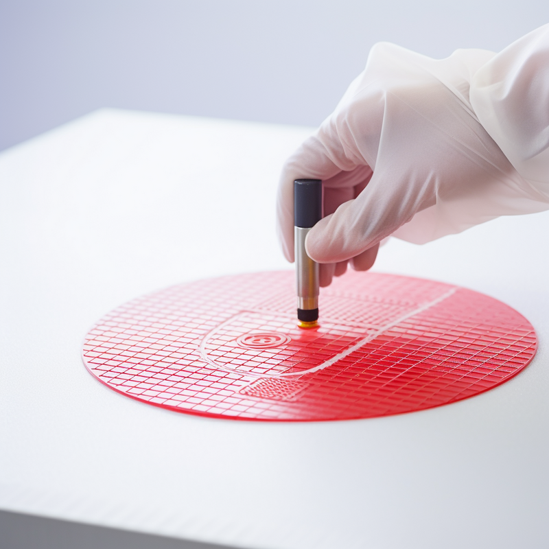
Nanoprinting is a cutting-edge technology that involves the precise fabrication of nanostructures on various substrates. This process allows for the creation of intricate patterns and designs at a nanoscale level, which is essential for a wide range of applications, including electronics, biotechnology, and materials science. Nanoprinting techniques utilize various methods such as inkjet, lithography, and nanoimprint lithography to achieve high-resolution patterning and control at the nanoscale. This technology holds great promise for the development of advanced devices and materials, paving the way for new breakthroughs in nanotechnology and its impact on different industries.
Advanced nanoprinting techniques play a crucial role in various fields such as nanoelectronics, smart materials, and biomedical devices. These techniques are essential for creating precise and intricate nanostructures, which are key components in the development of advanced technologies and devices.
In nanoelectronics, advanced nanoprinting techniques enable the fabrication of nanoscale features on semiconductor materials, leading to the production of high-performance electronic devices with improved efficiency and functionality. In the field of smart materials, nanoprinting allows for the precise patterning of nanomaterials, enabling the creation of smart coatings, sensors, and actuators with unique properties such as self-healing and shape memory. In biomedical devices, advanced nanoprinting techniques are used to create precise and customizable drug delivery systems, tissue engineering scaffolds, and diagnostic tools at the nanoscale, leading to advancements in personalized medicine and healthcare.
Examples of 3D nanoprinting applications include the fabrication of complex nanostructures for advanced photonics, the development of high-performance nanoscale sensors for scientific research, and the production of customized nanomaterials for commercial manufacturing. These applications have the potential to revolutionize scientific research and commercial manufacturing by enabling the creation of advanced materials and devices with unprecedented precision and functionality. Overall, advanced nanoprinting techniques have the potential to drive innovation and advancement in various fields, making them a critical area of research and development.
Nanoprinting techniques have revolutionized the field of nanotechnology by enabling the precise manipulation of materials on a nanoscale level. This has opened up new possibilities for creating advanced electronic, photonic, and biomedical devices. These techniques utilize a variety of methods and tools to accurately pattern and assemble nanoscale structures, offering enhanced control and precision. Understanding the background of nanoprinting techniques is crucial for appreciating the potential they hold for various applications in science and industry. This includes an understanding of the different methods and processes involved, as well as the materials and substrates used. By exploring the background of nanoprinting techniques, we can gain insight into how these advancements are shaping the future of nanotechnology and its impact on a wide range of disciplines.
Traditional 2D printing techniques include inkjet printing, laser printing, and offset printing.
Inkjet printing uses droplets of ink to create images on paper, and is commonly used for printing documents, photos, and small-scale advertising materials. This method is popular for its cost-effectiveness and ability to produce high-quality color prints, but it can be slower than other methods.
Laser printing uses a laser beam to produce high-quality text and graphics, and is commonly used for printing documents, reports, and marketing materials. This method is known for its speed, precision, and relatively low cost per page, but it is not as effective for large-scale printing as offset printing.
Offset printing involves transferring an inked image from a plate to a rubber blanket, then onto the printing surface. This method is suitable for high-volume printing of books, newspapers, and magazines due to its speed and cost-effectiveness, but it requires more setup time and has higher initial costs.
Each traditional 2D printing technique has its own advantages and limitations, making them suitable for various applications based on their process, technology, and capabilities.
The evolution of 3D printing technology has advanced rapidly, with the development of 3D nanoprinting systems playing a significant role. These systems have revolutionized the creation of intricate structures and optical devices at a nano-scale level. Advancements in 3D nanoprinting technology have led to the introduction of low-cost, easy-to-operate systems based on integrated fiber-coupled continuous-wave laser diodes. These systems have enabled researchers and scientists to fabricate high-resolution, complex nanostructures with precision and accuracy.
The potential for commercial manufacturing using 3D nanoprinting technology is vast. The accessibility of these systems to a wider range of scientists and researchers has opened up new possibilities for innovation and experimentation in various fields. The ability to create highly detailed optical devices and nanostructures has implications for a wide range of applications, from medical devices to telecommunications.
Overall, 3D nanoprinting technology has come a long way and continues to expand, offering exciting potential for commercial production and practical use in various industries. Its evolution has brought about new opportunities for creating intricate and precise structures at a nano-scale, making it a valuable tool for researchers and manufacturers alike.
Nanoprinting has seen significant advancements in recent years, with near-field electrospinning (NFES) being a particularly promising technique. NFES allows for the precise deposition of nanofibers on a substrate, enabling the fabrication of complex structures with fine features. Furthermore, the use of salt in NFES has been found to improve control over the deposition process, leading to more uniform and predictable patterns.
In addition to NFES, the development of a low-cost 3D nanoprinting system capable of printing metamaterials and optical devices has expanded the possibilities of nanoprinting. This system can create intricate structures with high precision, opening up new opportunities for applications in various fields.
Another exciting advancement in nanoprinting is the use of configured electric fields for programmable and parallel 3D nanoprinting, allowing for the simultaneous printing of multiple features with high resolution and accuracy.
Overall, these advanced nanoprinting techniques offer new possibilities for creating complex nanostructures with improved control and precision, paving the way for innovative applications in fields such as nanophotonics, microfluidics, and tissue engineering.
Direct laser writing techniques are advanced methods used to fabricate three-dimensional micro- and nanostructures with precision and accuracy. These techniques involve using a focused laser beam to directly write or modify the properties of a material, allowing for the creation of complex structures at a very small scale. This process is vital in the development of various applications, including photonics, microfluidics, and biomedical engineering. In this article, we will explore the different types of direct laser writing techniques and their applications in different fields. We will also discuss the advantages and limitations of using this technology and its potential to revolutionize the manufacturing industry.
Direct laser writing is a nanofabrication technique that involves using a focused laser beam to precisely write patterns or structures onto a substrate. This process enables the creation of high-resolution features at the nanoscale, making it an essential tool in the production of microdevices, photonic devices, and sensors.
The direct laser writing technique begins with a focused laser beam that is directed onto a photosensitive substrate, such as a polymer or glass. The intensity of the laser beam is modulated to control the exposure of the substrate, allowing for the precise writing of features at the nanoscale. Through this method, complex structures can be created with high precision and accuracy, making it a valuable tool in nanofabrication.
This technique has wide-ranging applications in various fields, including microelectronics, photonics, and biotechnology. It enables the rapid prototyping of microdevices and the fabrication of intricate photonic devices for optical communication and sensing. Overall, direct laser writing plays a crucial role in advancing nanofabrication technologies and facilitating the development of cutting-edge devices with high-resolution features.
Nanoprinting involves the precise deposition of materials at the nanoscale, and laser beams have become a key tool in this process. The development of a low-cost 3D nanoprinting system using a continuous-wave laser diode has allowed for the creation of arbitrary 3D structures with extremely fine features.
This technology utilizes laser beams to precisely control the movement and deposition of materials on a substrate, allowing for the creation of complex and detailed structures with high precision. The ability to create such fine features at the nanoscale opens up a wide range of potential applications in fields such as electronics, medicine, and materials science.
In electronics, nanoprinting with laser beams can be used to create intricate circuitry and components at the nanoscale, enabling the development of smaller, more efficient devices. In medicine, this technology could be used to create precise drug delivery systems or tissue scaffolds. In materials science, nanoprinting with laser beams could be applied to create advanced materials with tailored properties.
Overall, the use of laser beams in nanoprinting has the potential to revolutionize various industries by enabling the creation of complex 3D structures at the nanoscale with unprecedented precision and efficiency.
 Author: Dave Smiley